Huawei Silkroad Electronic Technology Co., Ltd.
- Sales manager:Mr. Liu
- Mobile/WhatsApp:+86 15931673319
- Address: East of Baimiao Village, Beiqijia Town, Changping District, Beijing

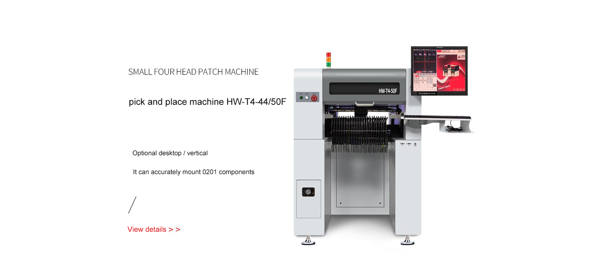
author: click::341 Publication time:2022-07-20
A, required documents 1, BOM list component list 2, no soldering list 3, SMT coordinate file 4, device schematic diagram 5, manually soldered device list 6, PCB two for making stencil files, instructions for making steps and methods for each file 1, BOM list component list 2, non-soldering list 3, SMT coordinate file 4, product silkscreen diagram (recommended to be made in DXP) (1), top parameter diagram (2), top number diagram (3), Bottom surface parameter diagram (4), bottom parameter diagram 5, manual welding device list 6, PCB plate steel mesh file professional to undertake the research and development of new productSMT patch proofing.PCBA sample patch.
BGA patch welding.No engineering fee, start-up fee, steel mesh fee, courier fee, price is preferential than the factory 70%, welcome to consult 13686458285 Tangsheng official website:/Three, the steps and methods of each file production detailed description 1, BOM list component list production method: export and then organize in the schematic can be exported method: in protel and DXP inside the same method, it is recommended to export in DXP in the interface to select [Reports/BillofMaterial], and then directly select Next until Finish as shown in figure: 2, Do not solder the list according to the first step of the component list can be sorted out 3, SMT coordinate file export methods and steps: (1), select [File/Open...] Open a. PCB files; (2) Click TopLayer and select [Edit/Select/AllonLayer] layer on all; (3) Click BottomLayer and select [Edit/Select/AllonLayer] layer on all; (4) After completion, press Shift+Delete to delete the excess lines of the Top surface and the Bottom surface; (5) Select [Design/Options...], open the Layers button, check [Toplayer]/[BottomLayer] under BasicLayers, then check [TopOverlay]/[BottomLayer] under Silkscreen, and then check [Keepout] under Other; Note: It is also possible to turn off Top and Bottom separately, which is more clear and concise. (6) After completing the above steps, you can clearly display the pad screen printing position map; (7) Select [Edit/Origin/Set] to set the origin position (after the PCB origin position is set, the PCB origin position remembered on the machine should also be set here); (8) Select [File/CAMManager.] In the Export Wizard, select PickPlace, tick Text, keep clicking Next, select Metric Metric in units, finish generating a PickPlace file, check press F9GenerateCAMfiles; (9) CAMfor in the left [Explorer] window: Locate PickPlace under the directory: File, right-click to export to the destination path you want; (10), then open this PickPlace file in Excel and organize it into files required by SMT, where MidX and MidY are the X and Y coordinates required by SMT. Note: TopLayer and BottomLayer should be separated when sorting 4, product component position silkscreen print pdf document (recommended to be made in DXP) (1), top surface parameter diagram top surface parameter diagram that is, TopOverlay layer resistance, capacitance, IC resistance value, capacitance, IC name, etc. (10K, 1UF. MAX354, etc.) Note: Each parameter is best centered (within the pad silk screen) Steps and methods: A, open a PCB file B in the DXP, select Only Show TopOverlay and KeepOutLayerC, hide the device number, only display the device parameters, place the parameters of each device within the pad silk screen, put it in the middle, pay attention to the consistency of neatness and direction D, select [File/SmartPDF ...] Export to PDF file detailed as follows Direct next step until completion Key steps as shown in the following figure: Patch Screen Diagram Export Steps Patch Screen Diagram Export Step Patch Screen Diagram Export Step Note: Figures 2, 3, 4 indicate that select only output TopOverlay and KeepOutLayer layers left mouse button to select layers, right mouse button to select delete layers and add layers Delete to delete layers; InsertLayer for adding layers (2), top number diagram top surface number diagram that is, TopOverlay layer resistance, capacitance, IC number (R1, C1, U1, etc.) Note: Each number is best centered (within the pad silk screen) Steps and methods: A, open a PCB file B in DXP, choose to display only TopOverlay and KeepOutLayerC, hide device parameters, only display device number, Place the number of each device within the pad screen, place it in the middle, pay attention to the consistency of neatness and orientation, and select [File/SmartPDF...] Exporting to a PDF file is detailed as in the first step above (3), the bottom parameter diagram The bottom parameter diagram is the PottomOverlay layer each resistance, capacitance, and capacitance Resistance value, capacitance value, IC name, etc. of ic (10K, 1UF. MAX354, etc.) Note: Each parameter is best centered (within the pad silk screen) Steps and methods: A, open a PCB file B in DXP, select only show BottomOverlay and KeepOutLayerC, hide the device number, only display the device parameters, place the parameters of each device within the pad silk screen, put in the middle, pay attention to the consistency of neatness and direction D, select [File/SmartPDF... ] Export to PDF file Detailed steps are basically the same as the first step above The difference is that only the output OfbotOverlay and KeepOutLayer are selected, as shown in the following figure: SMT Silkscreen Diagram Export Step (4), Bottom Surface Parameter Diagram Bottom Number Diagram That is, The Number of Each Resistor, Capacitor, IC of the PottomOverlay Layer (R1, C1, U1, etc.) Note: Each number is best centered (within the pad screen) Step and method: A, Open a PCB file B in DXP, select Show only BottomOverlay and KeepOutLayerC, hide the device parameters, display only the device number, place the number of each device within the pad silkscreen, put it in the middle, pay attention to the consistency of neatness and orientation D, select [File/SmartPDF...] Export to PDF file details as in the third step above 5, manually solder the device list according to the BOM list can be sorted out 6, PCB plate stencil file This file is provided by the hardware department